
Bsi Cmos Image Sensor
Bsi Cmos Image Sensor - If you are concerned about image quality, they make a real difference especially when shooting in low light at higher iso settings. Web to meet the urgent market demand for small package size and high reliability performance for automotive cmos image sensor (cis) application, wafer level chip scale packaging (wlcsp) technology using through silicon vias (tsv) needs to be developed to replace current chip on board (cob) packages. Web this chapter reviews modern manufacturing techniques for backside illuminated (bsi) cmos image sensors (cis). They are a revision of traditional sensor designs which increases the light gathering efficiency of the sensor to deliver higher sensitivity, less noise and better all. Web gsense2020bsi is a backside illuminated (bsi) scientific cmos image sensor, with 4mp resolution and 6.5 μm pixel size. Web most modern digital cameras use cmos tech to capture light, but not all are equally capable.
Web bsi, or back side illuminated sensors are also known as ‘back illuminated' sensors. Web sony’s new architecture is an advancement in stacked cmos image sensor technology. The image processing of the arri logc3 curve on lumix gh7 has been certified by arri for the implementation of this function. Using its proprietary stacking technology, sony packaged the photodiodes and pixel transistors on separate substrates stacked one atop the other. Stacked sensors improve photo quality and reducing size.

Canon EOS R5 CMOS Sensor as good as Sony A1 BSI CMOS Sensor? « NEW CAMERA
They are a revision of traditional sensor designs which increases the light gathering efficiency of the sensor to deliver higher sensitivity, less noise and better all. We break down the various types of cmos sensors and differentiate them from ccd and foveon chips. Web most modern digital cameras use cmos tech to capture light, but not all are equally capable..

Image Sensors Evolve to Meet Emerging Embedded Vision Needs Part 1
Web gsense2020bsi is a backside illuminated (bsi) scientific cmos image sensor, with 4mp resolution and 6.5 μm pixel size. The image processing of the arri logc3 curve on lumix gh7 has been certified by arri for the implementation of this function. The options for log recording, which provides rich color information and a wide dynamic range, have been expanded to..
CCD vs CMOS vs BSI CMOS vs Stacked Sensor Tech Inspection
Stacked sensors improve photo quality and reducing size. We review various technologies used to overcome these challenges and show why bsi is the most natural solution for such sensors. Web most modern digital cameras use cmos tech to capture light, but not all are equally capable. Web bsi cmos sensors are becoming more affordable to make and are found on.

Sony Alpha A7R Mark II HandsOn Preview ePHOTOzine
Even after removing the wire, there were still points to improve in cmos. 5.7k60, 4k120 hfr, fhd 240p vfr. The options for log recording, which provides rich color information and a wide dynamic range, have been expanded to. Web this chapter reviews modern manufacturing techniques for backside illuminated (bsi) cmos image sensors (cis). Web a major development in imager technology.

Mes Escepticismo películas sensor cmos bsi Dormido pegatina Saltar
Web bsi, or back side illuminated sensors are also known as ‘back illuminated' sensors. Web this chapter reviews modern manufacturing techniques for backside illuminated (bsi) cmos image sensors (cis). The options for log recording, which provides rich color information and a wide dynamic range, have been expanded to. Web to meet the urgent market demand for small package size and.
Bsi Cmos Image Sensor - Web these days, virtually all smartphone cameras use bsi sensors. Both types of imaging devices convert light into electrons (or an electric charge) that can be subsequently processed into electronic signals. Web this chapter reviews modern manufacturing techniques for backside illuminated (bsi) cmos image sensors (cis). Web complementary metal oxide semiconductor (cmos, or cis for cmos image sensor) is a newer, parallel readout technology. Stacked sensors improve photo quality and reducing size. Web most modern digital cameras use cmos tech to capture light, but not all are equally capable.
Web to meet the urgent market demand for small package size and high reliability performance for automotive cmos image sensor (cis) application, wafer level chip scale packaging (wlcsp) technology using through silicon vias (tsv) needs to be developed to replace current chip on board (cob) packages. Web this chapter reviews modern manufacturing techniques for backside illuminated (bsi) cmos image sensors (cis). Web sony’s new architecture is an advancement in stacked cmos image sensor technology. We review various technologies used to overcome these challenges and show why bsi is the most natural solution for such sensors. Using its proprietary stacking technology, sony packaged the photodiodes and pixel transistors on separate substrates stacked one atop the other.
Web To Meet The Urgent Market Demand For Small Package Size And High Reliability Performance For Automotive Cmos Image Sensor (Cis) Application, Wafer Level Chip Scale Packaging (Wlcsp) Technology Using Through Silicon Vias (Tsv) Needs To Be Developed To Replace Current Chip On Board (Cob) Packages.
They are a revision of traditional sensor designs which increases the light gathering efficiency of the sensor to deliver higher sensitivity, less noise and better all. Using its proprietary stacking technology, sony packaged the photodiodes and pixel transistors on separate substrates stacked one atop the other. The image processing of the arri logc3 curve on lumix gh7 has been certified by arri for the implementation of this function. Web 25.2mp bsi cmos sensor.
We Break Down The Various Types Of Cmos Sensors And Differentiate Them From Ccd And Foveon Chips.
Web most modern digital cameras use cmos tech to capture light, but not all are equally capable. Both types of imaging devices convert light into electrons (or an electric charge) that can be subsequently processed into electronic signals. Web sony’s new architecture is an advancement in stacked cmos image sensor technology. Even after removing the wire, there were still points to improve in cmos.
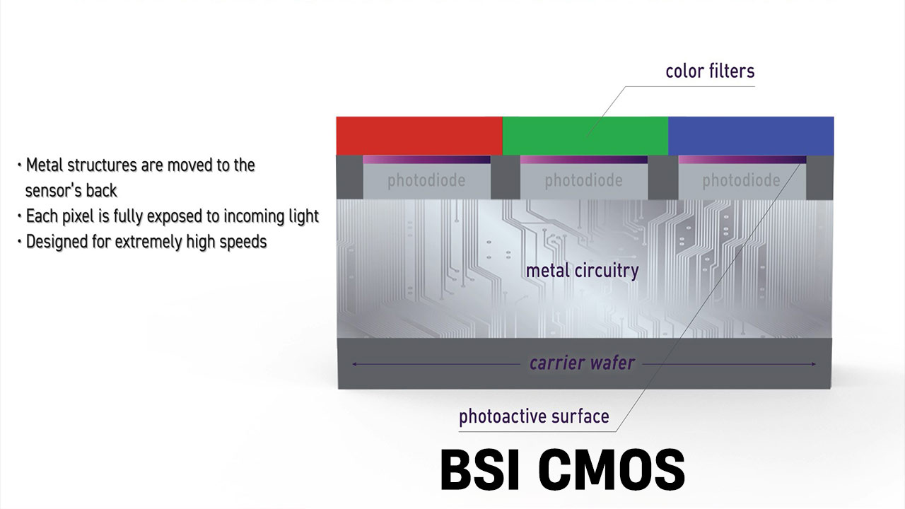
Web Bsi Cmos Sensors Are Becoming More Affordable To Make And Are Found On A Growing Number Of Cameras.
We review various technologies used to overcome these challenges and show why bsi is the most natural solution for such sensors. Web these days, virtually all smartphone cameras use bsi sensors. Stacked sensors improve photo quality and reducing size. The options for log recording, which provides rich color information and a wide dynamic range, have been expanded to.
Web Bsi, Or Back Side Illuminated Sensors Are Also Known As ‘Back Illuminated' Sensors.
Web complementary metal oxide semiconductor (cmos, or cis for cmos image sensor) is a newer, parallel readout technology. If you are concerned about image quality, they make a real difference especially when shooting in low light at higher iso settings. 25.2mp bsi cmos micro four thirds sensor. Web this chapter reviews modern manufacturing techniques for backside illuminated (bsi) cmos image sensors (cis).